
Process · Coating Inspection
Automatically inspect conformal coating on PCBs
Automated coating inspection checks the result after selective conformal coating. Cameras and coordinated lighting help detect missing, excessive or splashed coating and document inspection results in a traceable form.
What conformal coating inspection evaluates.
The inspection compares captured images with a configured inspection program. UV and white light reveal different features. The CI-900 uses a 20-megapixel camera together with colour and image comparison.
The system is specified for optical inspection of conformal coatings. This does not imply general solder-joint inspection or inspection of hidden areas. Actual inspection capability depends on coating, fluorescence, geometry, lighting and the agreed reference samples.
Typical inspection tasks.
Detect missing coating
Specified coating areas are checked for visible gaps or incomplete coverage.
Evaluate excessive coating
Oversized or unwanted coating areas can be assessed against defined inspection regions.
Find splashes
Visible coating spots outside the target regions can be configured as a separate defect type.
From reference image to inspection result.
1. Define inspection areas
Target areas, exclusion zones and relevant defect types are defined for the assembly.
2. Capture images
The PCB is recorded under UV and white light. Components, coating and surface finish affect the image.
3. Evaluate and document
The inspection program compares the features. Statistical software supports searching and exporting results.
Selection criteria for automated coating inspection.
Coating and fluorescence
The material must be distinguishable under the selected illumination. Coating type and coating appearance therefore belong in application trials.
Component height and shadows
Tall components, connectors and narrow gaps can hide relevant areas. Visibility must be assessed on the actual assembly.
Reference samples
Good and defective samples help separate acceptable variation from genuine defects.
Integration and data flow.
PCB, panel and carrier
The total transported format, including panel edge or workpiece carrier, must fit within the system range.
Line communication
The CI-900 is specified with SMEMA communication. Conveyor height, direction and transfers are coordinated with the existing line.
Handling inspection results
Define who confirms defects, how rework is handled and which data should be stored or exported.
CI-900 example system
Verified key data.
The technical values describe the CI-900. Detectability and limits are configured using the actual coating and representative assemblies.
- Camera
- 20-megapixel CMOS, top
- Pixel resolution
- 0.13 mm/pixel
- PCB format
- 50 × 50 to 450 × 450 mm
- Illumination
- UV and white light
- Evaluation
- Colour and image comparison
- Line communication
- SMEMA
Matching system.
View all technical data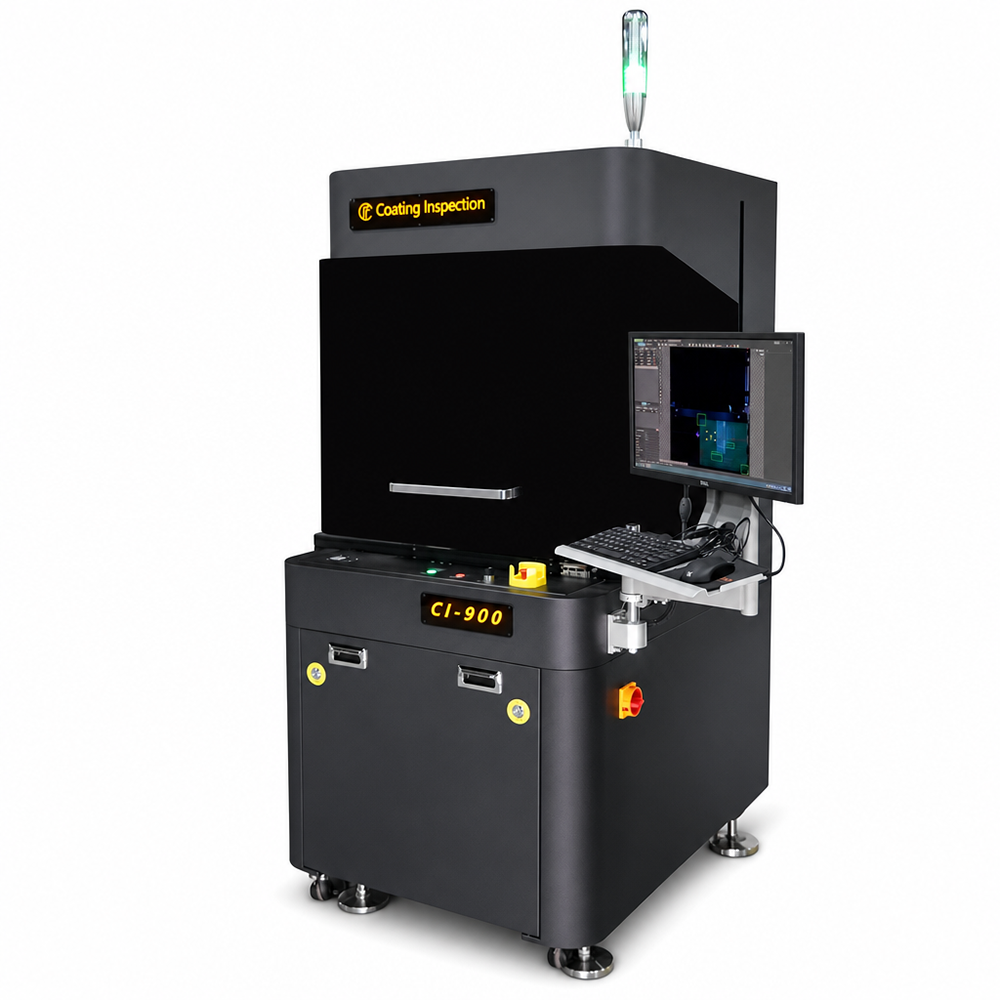
CI-900
Inline inspection system with 20-megapixel camera, UV and white light, statistics and export functions.
50 × 50 to 450 × 450 mm PCB formatInlineInformation needed for system planning.
Required inputs include assembly format, panel or carrier, coating designation, target regions, known defect types, good and defective samples, and conveyor and line-communication data.
Why reference samples matter.
Camera resolution alone does not define reliable defect detection. Representative samples show how coating, components, shadows and acceptable process variation appear in the image.
Frequently asked questions about coating inspection.
Which defects are specified for the CI-900?
The manufacturer information includes missing, excessive and splashed coating.
Does the system inspect solder joints?
The CI-900 is specified for optical inspection of conformal coatings. General solder-joint inspection should not be inferred from this description.
Is a high-resolution camera sufficient for reliable results?
No. Lighting, coating properties, component geometry, the inspection program and representative reference samples work together.
Define the inspection task.
Send us the assembly format, coating, target regions and representative defect examples.